Since Google made its first Tensor processor for Pixel devices, its chips have been manufactured by Samsung Foundry. After four generations, though, the company is ditching Samsung Foundry to go with TSMC to fabricate its next-generation Tensor chip, the Tensor G5, which will be used in the Pixel 10 series.
More information about Google’s switch to TSMC has been revealed.
Tensor G5 chip is made using TSMC’s 4nm process
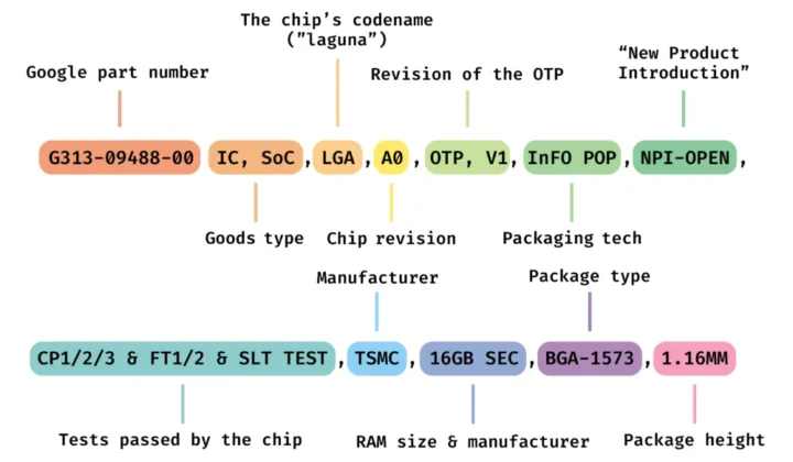
The information spotted by AndroidAuthority reveals that Google’s Tensor G5 chip, which will be used in the Pixel 10, is made by TSMC. As per a publicly available trade database, Google LLC has shipped a new chip from Taiwan to an Indian firm (called Tessolve Semiconductor) for testing. As you can see in the image below, the chip’s description reveals more details, including its internal codename, chip type, revision, tests passed, manufacturer, RAM, and more.
The Tensor F5 is codenamed ‘Laguna Beach,’ which has been known for a while and can be spotted as ‘LGA’ in the document. The chip is packaged using InFO POP (Integrated Fan-Out Package-On-Package), a chip packaging technology from TSMC. The chip description also mentions A0, which is the earliest revision available. SLT refers to system-level testing done using the chip, a process of using the chip in an actual test phone.
Moreover, TSMC’s name is also mentioned in the description, along with 16GB RAM manufactured by SEC (Samsung Electronics). The packaging type of the chip, BGA-1573, is also mentioned in the trade document. The Tensor G5 is 1.16mm thick, according to the information revealed in the document.
Is Google unhappy with Samsung Foundry’s performance?
For four years, Google worked closely with Samsung Electronics for its in-house chips. Early Tensor chips were largely based on high-end Exynos chips, with some bits designed by Google. However, with each passing year, Google made more customizations to its chips to integrate better NPUs, among other things.
These chips were designed with the help of Samsung’s System LSI arm and manufactured by Samsung Foundry. Tensor chips were good but nowhere as powerful as rivals from Apple, MediaTek, and Qualcomm. Moreover, they always had overheating issues and inefficient modems, which could be related to Samsung Foundry’s fabrication technologies.
It is widely known in the industry that Samsung Foundry’s fabrication is much cheaper than TSMC’s, but it has a few issues related to power consumption and efficiency. Hence, Google might have switched to TSMC’s 4nm process for the Tensor G5 chip, which will be launched next year as a part of the Pixel 10 series.
Watch our video below to know the performance difference between the Exynos 2400 and the Snapdragon 8 Gen 3.
While Samsung Foundry was the first in the industry to start making chips using a 3nm process, it hasn’t found any big-name clients for its 3nm process apart from Samsung’s own System LSI arm. The first prominent chip to be made using Samsung Foundry’s 3nm process is said to be the Exynos W1000 chip used in the Galaxy Watch 7, and it could be unveiled in the second half of this year.
The next-generation Exynos chip, designed for the Galaxy S25, is said to be using Samsung Foundry’s second-generation 3nm fabrication process (SF3). It could be unveiled early next year. It remains to be seen how much of an improvement Samsung managed to pull off with its newer process node.


